Cmos inverter Standard cmos circuits used for the cmos interface. (a) level shifters [overview] cmos inverter: definition, principle, advantages
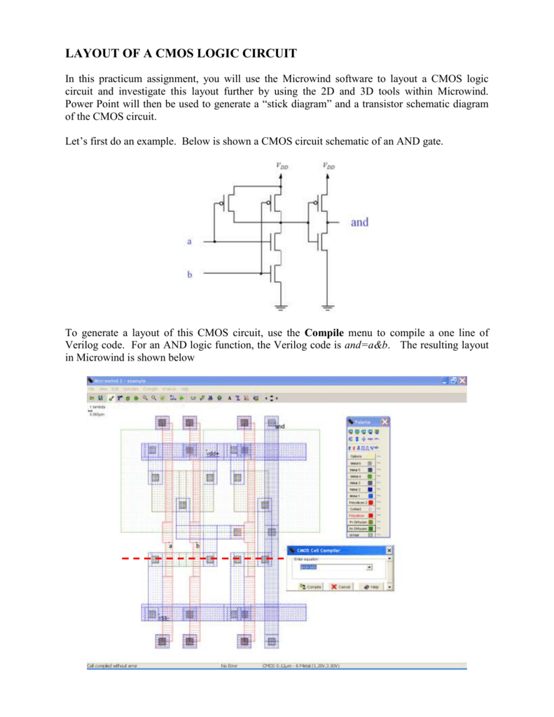
LAYOUT OF A CMOS LOGIC CIRCUIT
Cmos inverter circuit diagram principle minitool drain operation mosfet gate advantages definition general review resistors doesn makes contain any which
Draw a circuit diagram of a cmos inverter. draw its transfer
Xor cmos conventionalSchematic diagram of a cmos inverter. Cmos inverter circuit diagram draw explain its characteristics description transfer ques10Layout of a cmos logic circuit.
Cmos multiplexer mux transistors logic 2to1Cmos circuits shifters nano coupled Cmos circuit layout logicThe conventional cmos xor circuit [12]..
![[Overview] CMOS Inverter: Definition, Principle, Advantages - MiniTool](assets/kutukdev/images/placeholder.svg)
[solved] the cmos circuit shown below implements the function
.
.

![[Solved] The CMOS circuit shown below implements the function](https://i2.wp.com/storage.googleapis.com/tb-img/production/21/01/F9_Neha B_29-1-2021_Swati_D20.png)